 kingpdc




product search
search
“Ga2O3 on diamond” describes a material pair, but it does not tell you whether the oxide is crystalline, what interface was formed, or how effectively heat crosses that interface. A 2025 study of β-Ga2O3 on polycrystalline diamond is interesting precisely because it reports these questions separately—and shows why they should not be treated as interchangeable.
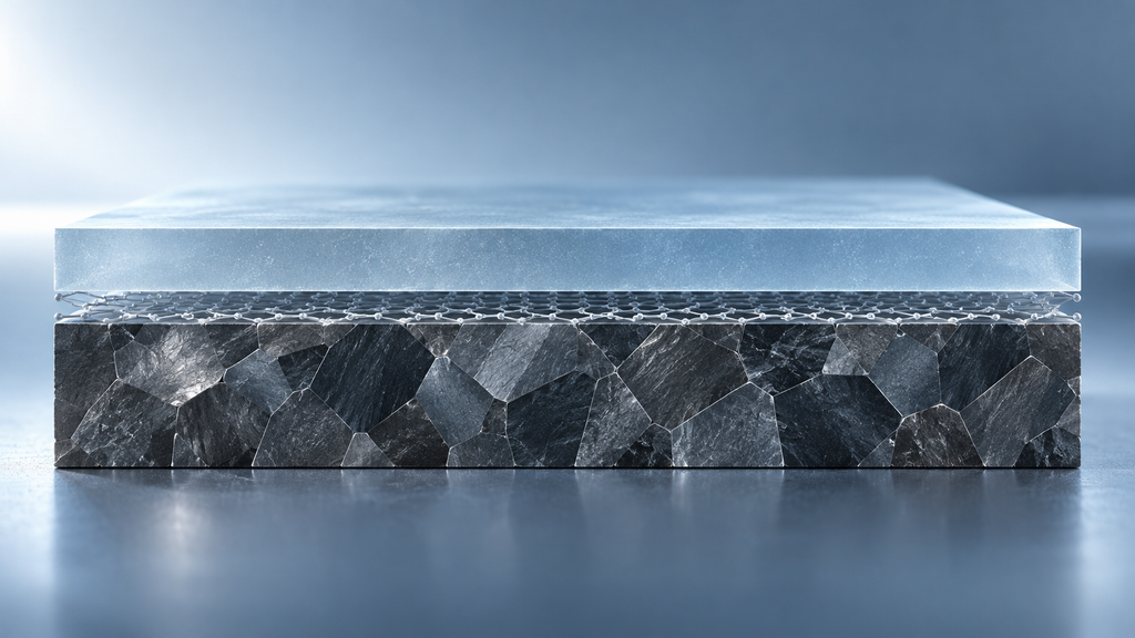
A 2023 atomic-layer-deposition study reported Ga2O3 films prepared on diamond. X-ray diffraction indicated that the deposited film was amorphous. The 2025 Nature Communications study addressed a different result: β-Ga2O3 grown on polycrystalline diamond using a single-layer graphene interlayer and mist chemical vapor deposition (mist-CVD). The distinction matters. The label “Ga₂O₃/diamond” alone does not establish that the oxide is crystalline β phase, nor does it reveal how the film was grown.
Polycrystalline diamond contains grains with different crystal orientations, making a uniform lattice relationship across the substrate difficult. In the 2025 work, graphene was introduced as a two-dimensional interlayer to modify the growth interface. The authors’ calculations favored a single graphene layer over thicker graphene, and transmission electron microscopy showed the β-Ga2O3/graphene/diamond interface in the fabricated samples.
The resulting oxide was predominantly oriented along (−201), but the paper also reported other orientations. That is a more precise description than calling the film single-oriented. The authors discuss lattice matching and oxygen surface density as factors in orientation, and report that oxygen conditions influence growth.
Under the tested conditions, the sample grown at 700 °C still showed an α-phase signal. At 760 °C, a 350 nm film reached a minimum (−201) rocking-curve full width at half maximum of 0.18°, with a root-mean-square surface roughness of 6.71 nm. X-ray photoelectron spectroscopy also showed a lower relative oxygen-vacancy contribution as oxygen flow increased. These are study-specific experimental results—not universal process settings that guarantee the same outcome on another tool or substrate.
Graphene had distinct effects on mechanical stress and heat transfer. Temperature-dependent Raman measurements indicated that the interlayer slightly relieved stress associated with the thermal-expansion mismatch between β-Ga2O3 and diamond. However, time-domain thermoreflectance (TDTR) did not show the graphene-containing samples to have the lowest effective thermal-boundary resistance.
For samples measured under the same β-Ga2O3 epitaxy conditions, the reported values were 2.82 m²·K/GW for the bare polycrystalline-diamond control, 6.08 m²·K/GW for single-layer graphene on diamond, and 6.02 m²·K/GW after oxygen-plasma treatment of the graphene/diamond interface. The 2.82 m²·K/GW value therefore belongs to the bare-diamond control—not to the graphene-interlayer sample.
The authors associate the higher resistance of the graphene interfaces with restricted phonon transport across the van der Waals interface, including limited real contact area and weaker adhesion. Plasma treatment introduced some covalent bonding and slightly reduced the measured resistance, but nonuniform treatment also led to random nucleation and somewhat lower film crystallinity and thermal conductivity. An interface can therefore help with stress while still imposing a thermal penalty.
The study also demonstrated a photodetector, reporting a photo-to-dark-current ratio of 106 and a responsivity of 210 A/W. The thermal conductivity reported for the 350 nm film was 7.19 W/(m·K). These figures describe the measured film, interface, and photodetector in that study. They are not high-power-transistor results, commercial product specifications, or evidence of volume-manufacturing capability.
Confirm whether a reported Ga2O3 layer is amorphous or crystalline β phase, and note the deposition method and thermal conditions. Similar material labels can describe materially different samples.
Thermal-expansion stress, thermal-boundary resistance, film thermal conductivity, and photodetector performance answer different questions. Compare like with like, and keep the substrate control group attached to its reported value.
The 2025 study shows that a graphene interlayer can support β-Ga2O3 growth with a preferred orientation on polycrystalline diamond and can slightly ease thermal-mismatch stress. It also shows that the interface may carry higher thermal-boundary resistance than the bare-diamond control. For design decisions, the useful takeaway is not simply that the materials can be combined; it is that phase, orientation, interface heat flow, and device performance must each be checked independently.
Diamond PDC Drill Bit Selection Guide. Utilizing Technical Skills To Reduce Procurement Costs.
View details
PDC Cutters—short for Polycrystalline Diamond Compact cutters—are at the heart of modern drilling efficiency. Built for strength and precision, these cutters feature a synthetic diamond layer fused onto a carbide base, allowing them to sl...
View details
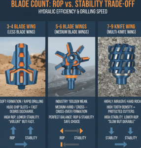
Master PDC Drill Bit Specifications: Body Type, Blade Count, Cutter Size & Hydraulic Design For Optimal ROP.
View details
Discover The Core Differences Between PDC And Tricone Bits. Learn Which Drill Bit Is Best For Your Formation.
View details